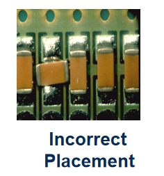
An in-circuit test (ICT) is a method used to test printed circuit boards (PCBs) to ensure that the assembled components are functioning correctly. It involves using a fixture or a bed of nails to make contact with various test points on the PCB. Here are some key aspects of an in-circuit test:
Component Verification: ICT checks that each component on the PCB is correctly placed and soldered. It verifies the presence, orientation, and value of components like resistors, capacitors, and integrated circuits.


Electrical Tests: It measures electrical properties such as resistance, capacitance, and inductance to ensure components are within specified tolerances.
Shorts and Opens Detection: The test can detect short circuits (unintended connections between traces) and open circuits (breaks in the circuit).
Functional Tests: In addition to static tests, ICT can also perform dynamic tests to check the functionality of certain components, such as integrated circuits and transistors.
Programming and Calibration: Some ICT systems can also be used to program components like microcontrollers and perform calibration tasks.
Test Coverage: ICT provides high test coverage, meaning it can test a high percentage of the possible faults in a PCB. This makes it very effective for quality control in PCB manufacturing.
Speed and Automation: ICT is typically automated and can test a board quickly, making it suitable for high-volume production environments.
Fixture-Based Testing: The test is performed using a custom fixture, often referred to as a bed of nails, which has spring-loaded pins that make contact with specific test points on the PCB.
ICT In-Circuit Test Platforms
Keysight 3073 Hardware Structure

Basic Keysight 3070 Test Process


Test Fixture In The System
Basic Test Fixture Concept

Test fixture Probe Working

What About The Tule Of Test Probe Implantation?
On the PCBA fixture lower probe test point requirements.
Today's electronic products are thinner and shorter, and PCB design and routing become more and more complex and difficult. In addition to functionality and safety, it must be producible and testable. We provide rules for testability requirements for design and wiring engineers, which, if noted, will save considerable fixture manufacturing costs and improve test reliability and fixture service life.
1. Although there are double-sided test fixtures, it is better to design and place the measured points on the same side. it is easier to test.
2. Priority of measured points:
A. Testpad
B. Component Lead
C. Through-hole (Via)
3. The distance between the two measured points or the measured point and the center of the pre-drilled hole shall not be less than 0.050"(1.27mm). More than 0.100"(2.54mm) is the best, followed by 0.075"(1.905mm).
4. The measured point should be at least 0.100" away from the nearby parts (located on the same side), if it is higher than 3m/m parts, it should be at least 0.120".
5. The measured points should be evenly distributed on the PCB surface to avoid high local density.
6. The diameter of the measured point is best not less than 0.035"(0.9mm), such as on the probe plate, it is best not less than 0.040"(1.00mm), and the shape of the square is better (the measured area is 21% higher than the circle). The measured points less than 0.030" need additional processing to direct the target.
7. The pad and Via of the measured points should not have a Solder Mask.
8. The measured point should be at least 0.100" away from the edge of the board or the edge of the fold.
9. PCB thickness should be at least 0.062"(1.35mm), PCB thickness less than this value is easy to bend, need special treatment.
10. The diameter of the Tooling Hole is best 0.125"(.3.175mm). The tolerance should be "+0.002"/-0.001". Its position should be on the opposite side of the PCB.
11. The position tolerance between the measured point and the positioning hole should be +/-0.002".
12. Avoid placing the measured point on the SMT parts, not only the measurable area is too small, unreliable, and easy to damage the parts.
Some tips on the PCB design and process for easy In-Circuit Test
No matter how shape the copper foil is, it is necessary to have a test point.
1. The order of consideration of the test points' position
ACI plug-in components are preferentially considered as test points.
To design the Copper foil, better put the solder tin on the copper foil.
Vertical parts plug-in dip comes after.
No Mask is allowed on the Via Hole.
2. Test Point Diameter
Over 1mm, The standard probes are compatible to test to achieve the correct test effect.
Below 1mm, It is better to apply the high precision test probe to match, it is high cost.
Make a good contact pad.
3. About the Shape of the Pad.
We accept any shape of pads, square, round, and arc. it is not limited.
4. Test Pitch
When designing the PCB, make an over 2mm test pitch if possible,
5. Demand on Double sides of the PCB
The single side PCB testing is preferred.
Via hole through the line to the dip side, so as to act as a test point and can be tested by the dip side.
It is necessary to lay the test pad beside the through hole when the Via hole is considered to be masked.
If it is not possible to make a single test side PCB, it will be made by a double-sided test fixture.
6. The testability of the empty foot should be considered within the allowable range. When there is no test point, the point must be put on.
7. It is better to have a jumper on the backup battery in the ICT test, it can effectively isolate the circuit.
8. Positioning hole requirements
Each piece of PCB shall have 2 positioning holes, and the holes shall not be stained with tin.
Select the diagonal and furthest two holes as positioning holes.
If you need any support fill in the blank to contact us for help.